Having dipped my toes in PCB design and manufacturing with the TentaOne, I figured it was time to tackle a project that I had my eyes on for a couple of years now.
Ever since I first saw the Dactyl in 2022, I’ve wanted to own a split keyboard. Not so much for the supposed ergonomic benefits, but more so because of the uniqueness and maker bragging rights.
The Goldilocks board
Split keyboards come in many flavours, with popular designs like the Sofle, Corne, etc. The common boards can be bought from some sellers and even prebuilt, but they’re quite costly.
The boards are often open source too, meant to allow you to send the boards to the fabrication houses yourself and even making your own changes.
At this point I figured, why not design my own board to fit in all the features I wanted?
Design
I started with a few design goals, and constraints.
I wanted a low profile board, with a number row and extra pinky column to allow for easier transitioning to a split keyboard. The extra keys would also allow options if I wanted to try different layouts, not limiting me from smaller layouts.
I was also pretty sold on ZMK from my positive experience with the TentaOne, which meant a wireless design.
The low profile keys were a major constraint as there are less options to choose from and there are no fixed standards. Choc v1s are nice because of their tighter spacing, but their unique stems means that its difficult to find keycaps. Additionally, it seems that the keycap stems are prone to breakage. Chocs are also quite expensive. I decided to go with Gateron low profile switches because I already use Gateron switches owing to them being comparatively cheaper. Additionally, Nuphy switches are also compatible with their hot swap sockets, offering options in the future. They aren’t a common option in the DIY keyboard space however, possibly because their sockets don’t reverse well, which I’ll touch on later.
The low profile design also meant that encoders wouldn’t fit well, so I didn’t include any. Instead I went with a carrying handle which I saw in another design and quite liked.
The most important manufacturing requirement for me, which will come in later, is that the components should be assembled by the PCB manufacturer where possible, saving me effort in the assembly and reducing the chance of errors. For the layout portion, this mostly meant that I could use SMD components which meant more flexibility in the component placement with less interference between components.
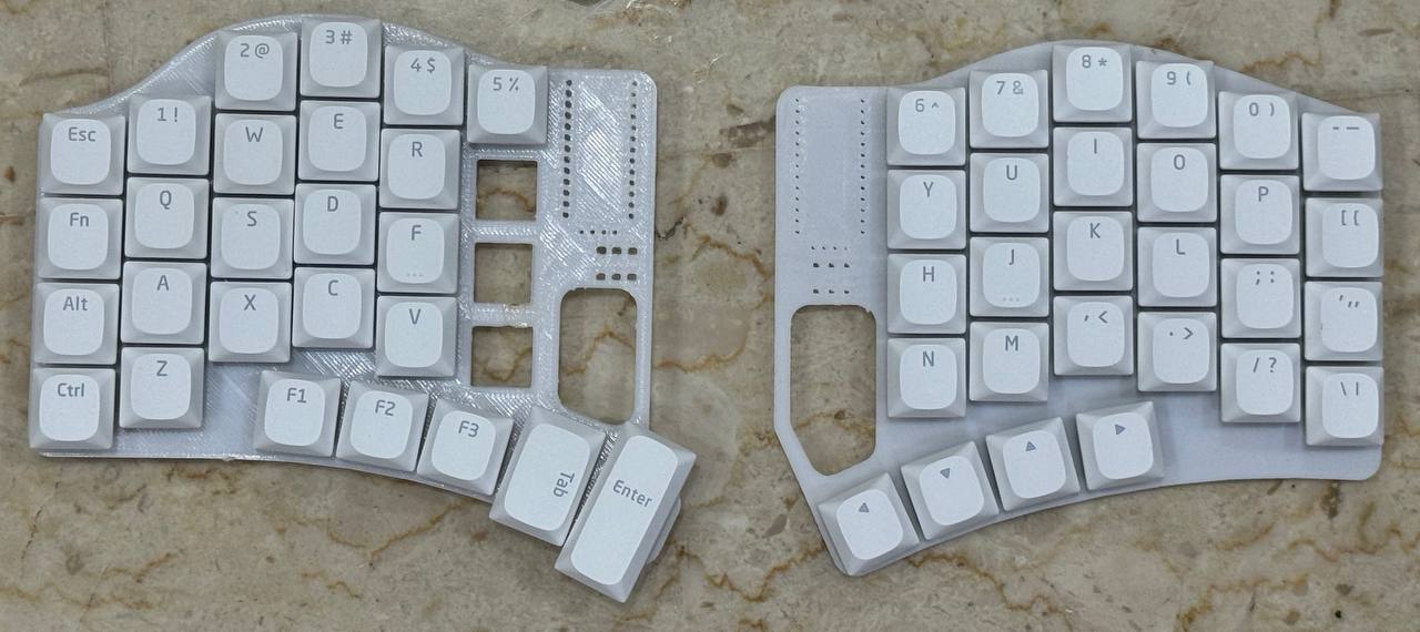
Another technique I liked was printing out layouts and cutting them out of cardboard to test the feel of the physical board. Instead of printer, however, I own a 3D printer and I figured it would be less finicky than cutting out keys from cardboard, so my prototypes were made of filament. Unfortunately, my printer isn’t the most reliable, resulting in a few printing mishaps, but I managed to get a layout I was happy with.
The result is an aggressive pinky stagger which feels comfortable in my hands’ typing position, a thumb key similarly in a comfortable resting spot plus one extra key to the left and right of it, plus two more just in case.
As an aside, I also tried out Ergopad, but I found it incredibly awkward to use.
Layout as Code
For the TentaOne, I used EasyEda because the component libraries from JLCPCB’s stock were easy to find and I had a lot of difficulty finding the symbols and footprints in other software. However, My experience with EasyEda for the TentaOne left me with a few pain points.
Firstly, it was difficult to lay out each individual component accurately on top of being extremely tedious. Secondly, the exported files weren’t very friendly with other software like Kicad and Onshape making me feel locked into the ecosystem.
To hopefully address these issue, I decided to try out Ergogen, having read FlatFootFox’s series of blog posts. Incidentally those posts are what inspired this one.
From here on out, I was mostly going in blind, which is why this blog post is more of a reflection than a tutorial.
Having already designed the layout in CAD, laying out the points for the left side was a breeze. I wasn’t sure how the mirroring would go, but I was more concerned if the entire workflow would pan out, so I pressed on with just the left side. The outlines also went fine, if a bit verbose. The PCBs were another story entirely, because the footprints I needed were not available on the web UI such as the switch footprints for my chosen switch and SMD components available.
As an aside, split keyboard designers don’t seem to like SMD components and assembly and I don’t quite understand why. It’s easier than having to solder the components yourself (they’re not shy from soldering SMD components by hand) and its generally easier to source the components from the manufacturer’s catalog (If any PCB manufacturer’s are reading this, I’m open to sponsorships for this project).
At this point I switched over to the Ergogen CLI which made it more difficult to view the points, but allowed me to add my own layouts and streamlined the PCB design phase.
PCB generation
The first order of business was preparing a footprint for my switches. Overall this was a rather straightforward, but it really helped me to appreciate teh code generation and text (lisp) based structure of Kicad PCB files.
A couple of points I took away from the process was the importance of the reference and value properties of the footprints.
The reference was important because defining the nets for the LEDs was a task I couldn’t figure out how to do in Kicad. The solution I found was to prepare a schematic in a Kicad project, move the generated PCB file into the project and update the PCB from the schematic, which would tie the symbols and their nets from the schematic to the PCB.
The value was important more so for the manufacturing because it made it easier for the manufacture’s web form to identify the right part for assembly.
The rest of the process was a rather repetitive process of preparing footprints and laying out components.
Routing
For the TentaOne, I didn’t give the thought of routing the PCB manually any time at all before heading to the auto router, with workable results.
Unfortunately Kicad doesn’t come with an auto router by default and freerouter didn’t settle on a solution after over 20k attempts, so I gave in and started manually routing the traces.
From my attempts so far, my takeaways are as follows:
- Route the important traces first. This means core features such as the keyboard matrix before the LEDs.
The key matrix is generally simpler to route and provides some constraints for the remaining routes. Doing the core features first also makes them less prone to having problems, meaning that even if the nice to haves don’t work, at least the keyboard should work.
- Use the ground plane and power plane for ground and power.
The per key LEDs and decoupling capacitors all need ground and power. Using traces to route them would be a major headache. Using the ground and power planes means that you just need to make sure that the planes are all joined together.
- Horizontal traces on one side and vertical traces on the other.
I’m still getting a feel of how to route more efficiently, but this seems to make sense in my head. This makes cutting traces easier as it should mean that you shouldn’t run up against traces on the same layer too often. I think adding the traces to a bus might also make it easier to cross. Additionally, the planes would be split more regularly, making it easier to connect them if they end up disconnected.
Mirroring
Now that I was confident I could manufacture half of the board, I decided to explore how Ergogen simplified generating the other half.
My reasoning for leaving it to this point is because I figured that even if only half worked, I could always just copy the layout into a second config for the right half.
On applying the mirror to the points, I immediately ran into an issue. The switch footprints were correct but the other components, mostly importantly the under pad vias (which truthfully could have been fixed in the routing) where rotated. I suppose this was minor considering that most importantly, the switch footprints were oriented correctly.
Nevertheless, some experimentation led me to understand that the mirroring only affected the translated or rotated components. While examples were space, reading the documentation and fiddling with the configs, I discovered the resist property which allowed me to use the same relative positions of the per key components on both sides of the board.
Manufacturing
Before mirroring the board, I had already uploaded some samples to figure out if it would be significantly cheaper to manufacture both halves together given the engineering costs, setup costs and part switching would not be duplicated. The combined board however incurred extra costs in terms of size.
My preliminary tests showed that it would be cheaper to combine both halves, and I figured it made sense, so I modified the original outline a little to accommodate it and added a v-cut. The result is as below.
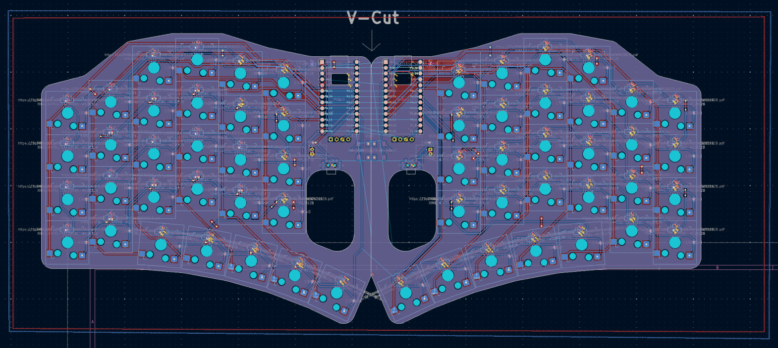
Unfortunately after submitted the board, I discovered that it was considered this as having multiple designs, incurring additional costs which put it at as much if not more than ordering the two halves separately. This put it as close to the same cost as ordering the halves separately.
I was already on the fence between submitting a combined or separate orders, but this tipped be back towards single orders.
The advantage of a single order would be that I could spend half the cost ensuring that the design worked, before going all in on both halves. On top of that it would allow more flexibility in changing up the designs for both halves, which is also one of the reasons I decided not to go for a reversable design. The other reasons were that I figured it would be simpler and more sensible to design the two halves in their optimal orientation rather than having tp have the layout owing to issues like which side to assemble and less than ideal pad placements etc. And I was thinking of having a silkscreen design on the back of the board.
As of the time of writing, what I have accomplished ends here, so stay tuned for part two which hopefully involves at least one finished half.